| Sign In | Join Free | My frbiz.com |
|
| Sign In | Join Free | My frbiz.com |
|
| Categories | Gallium Nitride Wafer |
|---|---|
| Brand Name: | zmkj |
| Model Number: | GaN-templates |
| Place of Origin: | CHINA |
| MOQ: | 5pc |
| Price: | by case |
| Payment Terms: | L/C, T/T |
| Delivery Time: | 2-4weeks |
| Packaging Details: | single wafer case in 100-grade cleaning room |
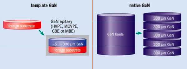
| Material: | GaN epi on Sapphire carrier |
| method: | HVPE |
| size: | 2inch |
| thickness: | 430um |
| industry: | LD,led,laser device,detector, |
| surface: | single side polished |
| Company Info. |
| SHANGHAI FAMOUS TRADE CO.,LTD |
| Verified Supplier |
| View Contact Details |
| Product List |
2inch GaN substrates template,GaN wafer for LeD,semiconducting Gallium Nitride Wafer for ld,GaN template, mocvd GaN Wafer,
III-Nitride(GaN,AlN,InN)Forbidden band width (light emitting and absorption) cover the ultraviolet,
visible light and infrared.GaN can be used in many areas such as LED display, High-energy Detection
and Imaging,Laser Projection Display, Power Device, etc.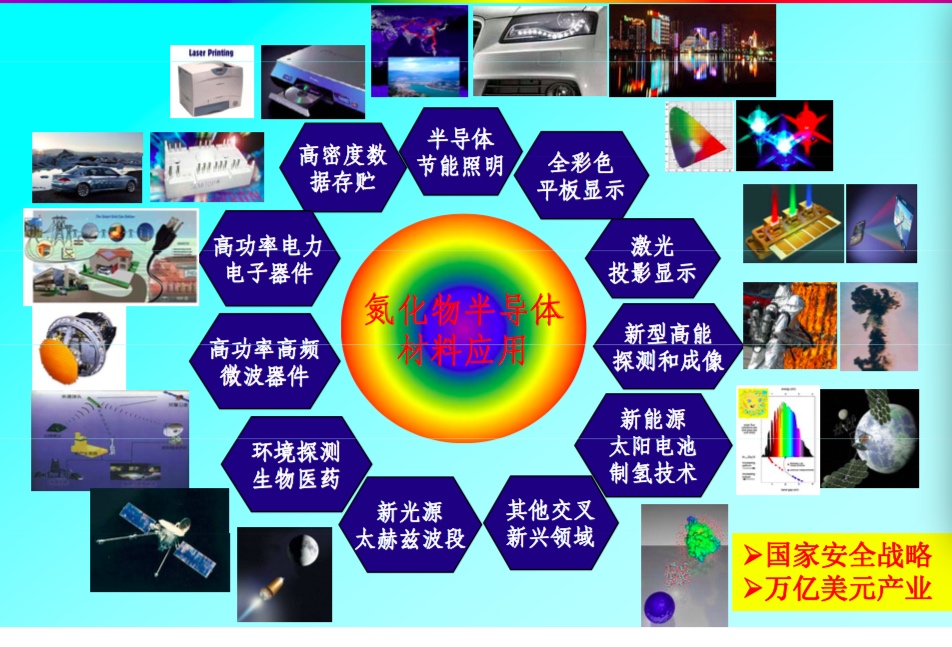
Specifications:
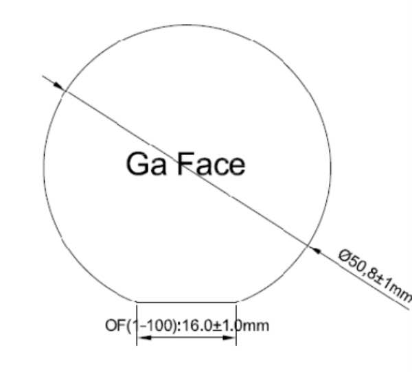
2” GaN Templates
Item | GaN-T-N | GaN-T-S |
Dimensions | Ф 2” | |
Thickness | 15 μm, 20 μm, 30 μm, 40 μm | 30 μm, 90 μm |
Orientation | C-axis(0001) ± 1° | |
Conduction Type | N-type | Semi-Insulating |
Resistivity(300K) | < 0.05 Ω·cm | >106 Ω·cm |
Dislocation Density | Less than 1x108 cm-2 | |
Substrate structure |
| |
Useable Surface Area | > 90% | |
Polishing | Standard: SSP Option: DSP | |
Package | Packaged in a class 100 clean room environment, in cassettes of 25pcs or single wafer containers, under a nitrogen atmosphere. | |
-FAQ –
Q: What you can supply logistics and cost?
(1) We accept DHL, Fedex, TNT, UPS, EMS, SF by FOB.
Q: What's the delivery time?
(1) For the standard products such as 2inch 0.33mm wafer.
For inventory: the delivery is 5 workdays after order.
For customized products: the delivery is 2 or 3 workweeks after
order.
Q: How to pay?
100%T/T In advance, Paypal, West Union, MoneyGram,

|
