| Sign In | Join Free | My frbiz.com |
|
| Sign In | Join Free | My frbiz.com |
|
| Categories | Piezoelectric Wafer |
|---|---|
| Brand Name: | CQT |
| Model Number: | LNOI Wafer |
| Certification: | ISO:9001, ISO:14001 |
| Place of Origin: | China |
| MOQ: | 10 pcs |
| Price: | $2000/pc |
| Payment Terms: | T/T |
| Supply Ability: | 50000 pcs/Month |
| Delivery Time: | 1-4 weeks |
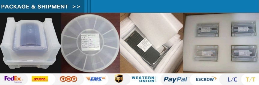
| Packaging Details: | Cassette/ Jar package, vaccum sealed |
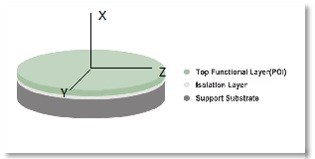
| Product: | LiNbO3 On Insulator |
| Diameter: | 4 inch, 6 inch |
| Top Layer: | Lithium Niobate |
| Top Thickness: | 300~600nm |
| Insolation: | SiO2 Thermal Oxide |
| Insolation Thickness: | 2000±15nm; 3000±50nm; 4700±100nm |
| the support layer: | Si、Fused silica |
| Application: | Optical Waveguides and Microwaveguides |
| Company Info. |
| Hangzhou Freqcontrol Electronic Technology Ltd. |
| Verified Supplier |
| View Contact Details |
| Product List |
4-Inch 6-Inch LNOI Wafers The Perfect Choice for Compact and High-Performance Optical Communication
Revolutionize Photonics with Ultra-Low-Loss LNOI Wafers
Next-Gen Lithium Niobate-on-Insulator (LNOI) Platform
Unlock unprecedented performance in integrated photonics with our
cutting-edge LNOI wafers, engineered for ultra-low optical loss and
sub-nanometer surface roughness . Combining stoichiometric LiNbO₃
thin films with thermally oxidized SiO₂ buried layers, our wafers
deliver >30x higher nonlinear efficiency than conventional bulk crystals, while enabling CMOS-compatible
fabrication.
Key Advantages
✓ Breakthrough EO Performance: Achieve >100 GHz modulation
bandwidth with r₃₃ >30 pm/V, ideal for 800G/1.6T coherent
transceivers.
✓ Quantum-Ready Precision: Custom periodic poling (PPLN) with
<5 nm domain error for entangled photon generation.
✓ Power-Hardened Design: Withstand >10 MW/cm² optical
intensity (Telcordia GR-468 certified).
Applications
▷ 5G/6G ultra-compact EO modulators
▷ Topological photonic circuits & optical computing
▷ Quantum frequency converters (C/L-band to telecom band)
▷ High-sensitivity LiDAR photodetectors
Technical Specifications
• Wafer Size: 100/150 mm diameter (2" to 6" customizable)
• LiNbO₃ Layer: X-cut/Z-cut, thickness 300±5 nm (standard)
• Buried Oxide: 1-3 μm SiO₂, breakdown voltage >200 V/μm
• Substrate: High-resistivity Si (>5 kΩ·cm)
| LNOI Wafer | |||
| Structure | LN / SiO2 / Si | LTV / PLTV | < 1.5 μm ( 5∗ 5 mm2 ) / 95% |
| Diameter | Φ100 ± 0.2 mm | Edge Exclution | 5 mm |
| Thickness | 500 ± 20 μm | Bow | Within 50 μm |
| Primary Flat Length | 47.5 ± 2 mm 57.5 ± 2 mm | Edge Trimming | 2 ± 0.5 mm |
| Wafer Beveling | R Type | Environmental | Rohs 2.0 |
| Top LN Layer | |||
| Average Thickness | 400/600±10 nm | Uniformity | < 40nm @17 Points |
| Refraction index | no > 2.2800, ne < 2.2100 @ 633 nm | Orientation | X axis ± 0.3° |
| Grade | Optical | Surface Ra | < 0.5 nm |
| Defects | >1mm None; ≦1 mm Within 300 total | Delamination | None |
| Scratch | >1cm None; ≦1cm Within 3 | Primary Flat | Perpendicular to +Y Axis ± 1° |
| Isolation SiO2 Layer | |||
| Average Thickness | 2000nm ± 15nm 3000nm ± 50nm 4700nm ± 100nm | Uniformity | < ±1% @17 Points |
| Fab. Method | Thermal Oxide | Refraction index | 1.45-1.47 @ 633 nm |
| Substrate | |||
| Material | Si | Orientation | <100> ± 1° |
| Primary Flat Orientation | <110> ± 1° | Resistivity | > 10 kΩ·cm |
| Backside Contamination | No visible stain | Backside | Etch |


|
