| Sign In | Join Free | My frbiz.com |
|
| Sign In | Join Free | My frbiz.com |
|
| Categories | Sapphire Wafer |
|---|---|
| Brand Name: | ZMSH |
| Model Number: | Sapphire Wafer |
| Place of Origin: | CHINA |
| Delivery Time: | 2-4 weeks |
| Payment Terms: | T/T |
| Material: | Al2O3 Monocrystalline |
| Diameter: | 50.80 mm |
| Thickness: | 430 um |
| Crystal Orientation: | A-plane |
| Surface: | Dsp |
| Bow: | ≤ 10 um |
| Company Info. |
| SHANGHAI FAMOUS TRADE CO.,LTD |
| Verified Supplier |
| View Contact Details |
| Product List |
Sapphire wafers, made from single-crystal aluminium oxide (Al2O3),
are prized for their exceptional hardness, thermal stability, and
optical properties. They are extremely scratch-resistant and
durable with a hardness rating of 9 on the Mohs scale. They have a
high flexural strength of up to 100,000 PSI, making them robust
under mechanical stress.
Thermally, sapphire wafers are stable up to their melting point of
2040°C and have a thermal conductivity of 25-35 W/(m·K) at room
temperature. Their low thermal expansion coefficient (5.3 x 10^-6
/K) ensures they remain stable across various temperatures, which
is crucial for high-temperature applications. They also possess
excellent electrical insulating properties with a dielectric
constant of 9.3 at 1 MHz and resistivity above 10^14 Ω·cm.
Optically, the thickness of 2-inch sapphire is 430um. These
sapphire wafers crystallographic orientations are A-plane (11-20).
They are precisely polished to achieve a surface roughness (Ra)
=0.8-1.2 um, ensuring superior optical clarity and performance.
These attributes make sapphire wafers essential in the
semiconductor, optics, and LED industries, providing robustness,
thermal and chemical stability, and exceptional optical clarity.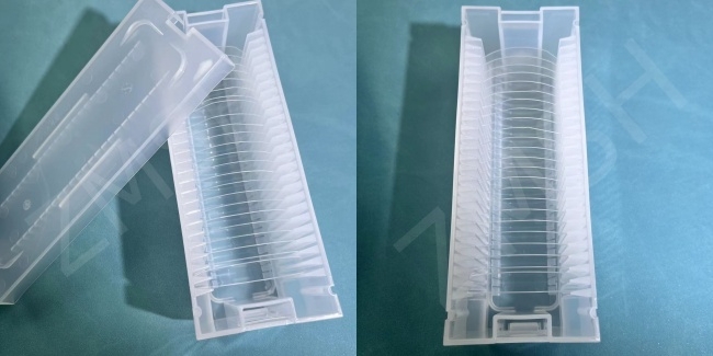
| Item | 2-inch A-plane(11-20) 430um Sapphire Wafers | |
| Crystal Materials | 99,999%, High Purity, Monocrystalline Al2O3 | |
| Grade | Prime, Epi-Ready | |
| Surface Orientation | A-plane(11-20) | |
| Diameter | 50.8 mm ± 0.1 mm | |
| Thickness | 430 um ± 25 um | |
| Primary Flat Length | 16.0 mm ± 1.0 mm | |
| Double Side Polished | Front Surface | Epi-polished, Ra < 0.5 nm (by AFM) |
| (DSP) | Back Surface | Epi-polished, Ra < 0.5 nm (by AFM) |
| TTV | ≤ 10 um | |
| BOW | ≤ 10 um | |
| WARP | ≤ 10 um | |
| Cleaning / Packaging | Class 100 cleanroom cleaning and vacuum packaging, | |
| 25 pieces in one cassette packaging or single piece packaging. | ||
Sapphire wafers are utilized in a variety of high-tech applications due to their unique properties such as hardness, thermal stability, and optical clarity. Here are some key applications:
LED Manufacturing:
Semiconductors:
Optical Windows:
Watch Crystals:
Medical Devices:


We offer customizable sapphire wafers tailored to your specific
requirements. Options include varying diameters (2”, 3”, 4”, 6”),
different crystallographic orientations (C-plane, A-plane,
R-plane), and precise thickness tolerances (±0.1 mm). Surface
finishes can be polished to achieve low surface roughness (Ra ≤ 0.3
nm). Additional features such as custom doping, laser marking, and
edge shaping are also available. These customizations ensure our
sapphire wafers meet the precise needs of applications in LED
manufacturing, semiconductors, optics, and more, providing optimal
performance and reliability.
Our Sapphire Wafer product technical support and services include:
- Material selection guidance to ensure optimal performance for
your application
- Custom sapphire wafer fabrication based on your specific
requirements
- Wafer cleaning and polishing services to remove surface defects
and impurities
- Quality control testing and analysis to ensure consistent wafer
performance
- Technical consultation to address any questions or concerns
regarding the use and handling of sapphire wafers
Q: How are sapphire wafers manufactured?
A: Sapphire wafers are produced using the Czochralski process, where
a seed crystal is dipped into molten aluminium oxide and slowly
pulled out while rotating to form a large boule. This boule is then
sliced into thin wafers using a diamond saw.
Q: How should sapphire wafers be handled and stored?
A: The following methods are just for reference.
Q: What are the environmental and safety considerations for
sapphire wafer production?
A: Please notice the ways followed sentences mentioned.

|
