| Sign In | Join Free | My frbiz.com |
|
| Sign In | Join Free | My frbiz.com |
|
| Categories | LiNbO3 Wafer |
|---|---|
| Brand Name: | BonTek |
| Model Number: | LiNbO3 |
| Place of Origin: | China |
| Certification: | ISO:9001 |
| MOQ: | 10 pcs |
| Price: | $500/pc |
| Supply Ability: | 300 pcs/month |
| Delivery Time: | 5-8 weeks |
| Packaging Details: | Cassette, Jar |
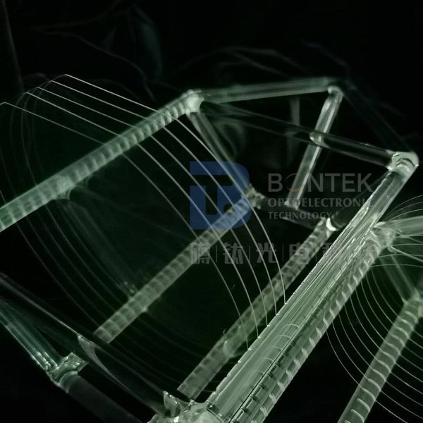
| Crystal: | LiNbO3 |
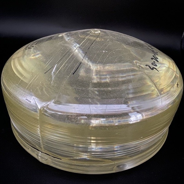
| Diameter: | 8 inch; Φ200mm |
| Orientation: | X-cut, Z-cut |
| Surface: | Polished |
| Surface Roughness: | Ra<0.5nm |
| Thickness: | 0.5mm, 0.7mm, 1mm |
| TTV: | <5um |
| Shape: | Round Wafer |
| Applications: | Optical Waveguides and Microwaveguides |
| Laser Marking: | Available as per request |
| Company Info. |
| Hangzhou Freqcontrol Electronic Technology Ltd. |
| Verified Supplier |
| View Contact Details |
| Product List |
8-inch LiNbO3 wafers refer to the specific size of LiNbO3 crystal substrates commonly used in the fabrication of optoelectronic devices and integrated circuits. These wafers are made from high-purity lithium niobate crystals and offer several advantages due to their larger size. Here is a description of 8-inch LiNbO3 wafers:
Increased Device Capacity: The larger surface area allows for a higher number of devices and integrated circuits to be fabricated on a single wafer, thereby improving production capacity and yield.
Enhanced Integration: With a larger area, 8-inch wafers enable higher device integration and improved performance due to the availability of more real estate for components and interconnects.
Improved Uniformity: The manufacturing process for larger wafers often results in better consistency and uniformity across the wafer, contributing to improved device performance and yield.
8-inch LiNbO3 wafers find applications in various fields where their unique optical and electro-optic properties are utilized. For example: Optical Modulators, Frequency Conversion, Acousto-Optic Devices, Integrated Optics, Nonlinear Optical Devices, Optical Sensors.
LiNbO3 Wafers should be packaged and shipped in accordance with the following guidelines:

|
