| Sign In | Join Free | My frbiz.com |
|
| Sign In | Join Free | My frbiz.com |
|
| Categories | Silicon Carbide Wafer |
|---|---|
| Brand Name: | ZMKJ |
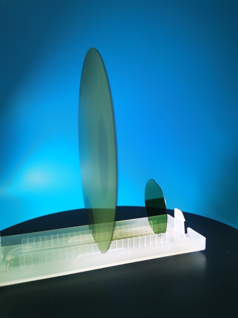
| Model Number: | 8inch sic wafers 4h-n |
| Certification: | ROHS |
| Place of Origin: | CHINA |
| MOQ: | 1pcs |
| Price: | by case |
| Payment Terms: | T/T, Western Union, MoneyGram |
| Supply Ability: | 1-20pcs/month |
| Delivery Time: | 3-6 months |
| Packaging Details: | single wafer package in 100-grade cleaning room |
| Material: | SiC single crystal |
| Grade: | Production Grade |
| Delivery date: | 3 months |
| Application: | device maker polishing test MOS |
| Diameter: | 200±0.5mm |
| MOQ: | 1 |
| Company Info. |
| SHANGHAI FAMOUS TRADE CO.,LTD |
| Verified Supplier |
| View Contact Details |
| Product List |
SiC Substrate/Wafers (150mm, 200mm) Silicon Carbide Ceramic Excellent CorrosionSingle crystal single side polished silicon wafer sic wafer polishing wafer manufacturer Silicon Carbide SiC Wafer 4H-N SIC ingots/200mm SiC Wafers 200mm SiC Wafers
About Silicon Carbide (SiC)Crystal
Silicon carbide (SiC), or carborundum, is a semiconductor containing silicon and carbon with the chemical formula SiC. SiC is used in semiconductor electronics devices operating at high temperatures, high voltages, or both. SiC is also one of the important LED components, it is a popular substrate for growing GaN devices and serves as a heat spreader in high-power LEDs.
| Property | 4H-SiC, Single Crystal | 6H-SiC, Single Crystal |
| Lattice Parameters | a=3.076 Å c=10.053 Å | a=3.073 Å c=15.117 Å |
| Stacking Sequence | ABCB | ABCACB |
| Mohs Hardness | ≈9.2 | ≈9.2 |
| Density | 3.21 g/cm3 | 3.21 g/cm3 |
| Therm. Expansion Coefficient | 4-5×10⁻⁶/K | 4-5×10⁻⁶/K |
| Refraction Index @750nm | no = 2.61 ne = 2.66 | no = 2.60 ne = 2.65 |
| Dielectric Constant | c~9.66 | c~9.66 |
| Thermal Conductivity (N-type, 0.02 ohm.cm) | a~4.2 W/cm·K@298K c~3.7 W/cm·K@298K | |
| Thermal Conductivity (Semi-insulating) | a~4.9 W/cm·K@298K c~3.9 W/cm·K@298K | a~4.6 W/cm·K@298K c~3.2 W/cm·K@298K |
| Band-gap | 3.23 eV | 3.02 eV |
| Break-Down Electrical Field | 3-5×10⁶V/cm | 3-5×10⁶V/cm |
| Saturation Drift Velocity | 2.0×10⁵m/s | 2.0×10⁵m/s |
To overcome these challenges and obtain high quality 200mm SiC
wafers,solutions are proposed:
In terms of 200mm seed crystal preparation, appropriate temperature
field, flow field, and expanding assemblwere studied and designed
to take into account crystal quality and expanding size; Starting
with a 150mm SiCseed crystal, carry out seed crystal iteration to
gradually expand the SiC crystal size until it reaches
200mm;Throuch multiple crystal growth and processing, gradually
optimize the crystal quality in the crystal expandingarea, and
improve the quality of 200mm seed crystals.
n terms of 200mm conductive crvstal and substrate preparation.
research has optimized the temperature fieland flow field design
for large size crystal growth, conduct 200mm conductive SiC crystal
growth, and controldoping uniformity. After rough processing and
shaping of the crystal, an 8-inch electrically conductive
4H-SiCingot with a standard diameter was obtained. After cutting,
grinding, polishing, processing to obtain SiC 200mmwafers with a
thickness of 525um or so.


Due to SiC physical and electronic properties, Silicon Carbide-based devices are well suitable for short wavelength optoelectronic, high temperature, radiation resistant, and high-power/high-frequency electronic devices, compared with Si and GaAs-based device.
SiC-based devices are
low lattice mismatch fall-nitride epitaxial layers
high thermal conductivity
monitoring of combustion processes
all sorts of UV-detection
Due to SiC material properties, SiC-based electronics and devices can work in very hostile environments, which can work under high temperatures, high power, and high radiation conditions

|
