| Sign In | Join Free | My frbiz.com |
|
| Sign In | Join Free | My frbiz.com |
|
| Categories | LiNbO3 Wafer |
|---|---|
| Brand Name: | zmkj |
| Model Number: | LT-001 |
| Place of Origin: | CHINA |
| MOQ: | 25pcs |
| Price: | by case |
| Supply Ability: | 5000pcs/month |
| Delivery Time: | 15-30days |
| Packaging Details: | PET Films or 25pcs casstle case by 100 grade cleaning room |
| materials: | LT LN single crystal |
| industry: | semiconductor wafer,saw wafer,optical wafer |
| application: | 5G,SAW device,optical glass, |
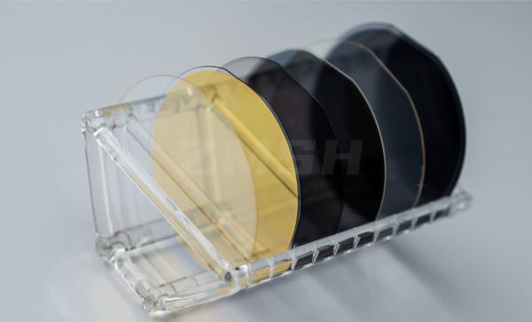
| color: | yellow, red,black |
| size: | 4inch |
| orientation: | Y-42° commen |
| Company Info. |
| SHANGHAI FAMOUS TRADE CO.,LTD |
| Verified Supplier |
| View Contact Details |
| Product List |
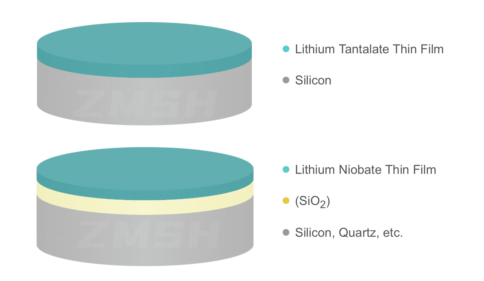
LiTaO3 LiNbO3 Wafers LN LT Thin Films Wafers 42°Y
LT & LN Wafer
The basic principle of SAW devices is the generation of elastic surface waves from electrical signals and their reconversion. The substrate material is a piezoelectric crystal such quartz (SiO2), lithium tantalate (LiTaO3) or lithium niobate (LiNbO3). This are single crystal materials, which are cut out after the growth process with a defined orientation to a wafer. NQW produced this wafer for SAW manufacture and R&D centres. Please find below typical specification requirements.
Application
Mainly used in photoelectric and other fields
Specification
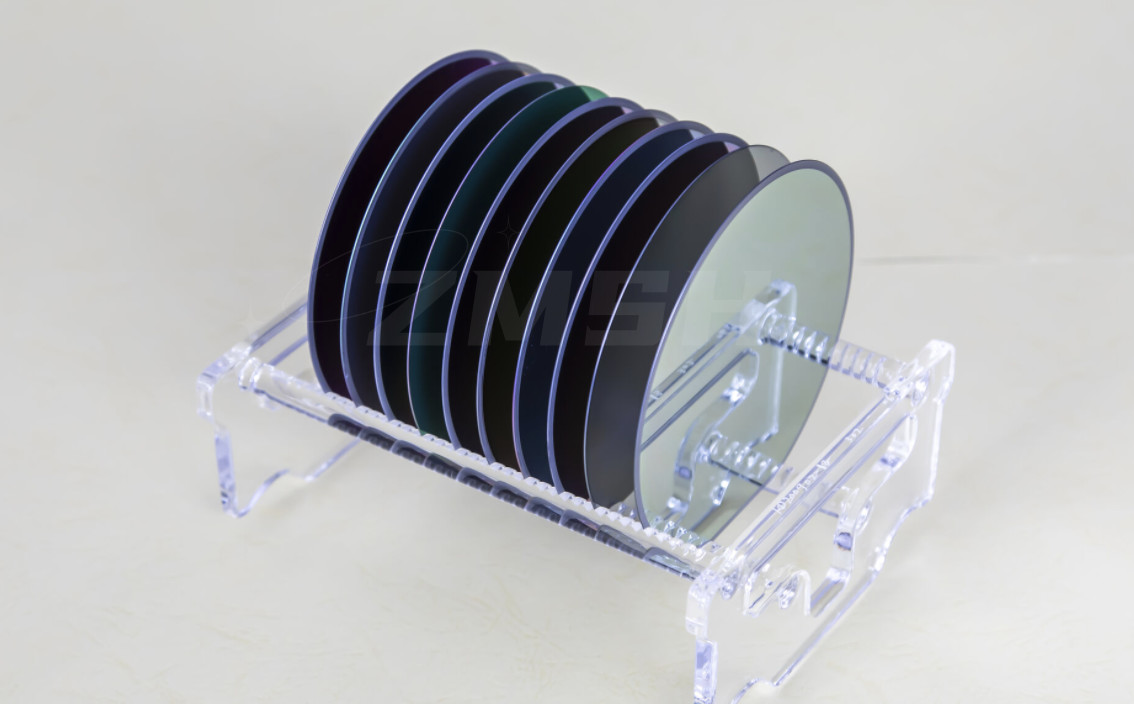
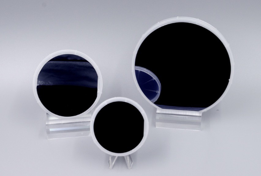
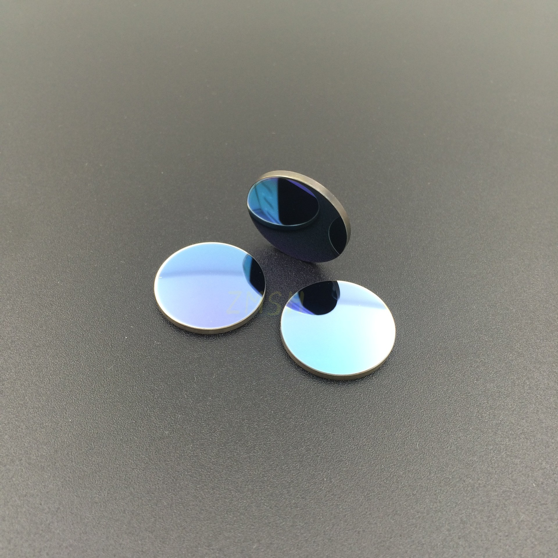
Product display
Related products
GaAs wafer
Ge wafer
FAQ
Q. Do you have any stock of wafer or ingots?
yes,aslike 3inch,4inch commen size substrates wafers are in stocks.
Q. Where is your company located?
Our company located in shanghai,China. factory is in wuxi city.
Q. How long will take to get the products?
Generally it will take 1~4 weeks to process and then delivery.
It is depend on the quantity and the size of the products.
Q: How about pay term & delivery ?
T/T 50%deposit and left part before delivery by FOB .
|
