| Sign In | Join Free | My frbiz.com |
|
| Sign In | Join Free | My frbiz.com |
|
| Categories | PCB Assembly Prototype |
|---|---|
| Brand Name: | HNL-PCBA |
| Model Number: | PCB Assembly06 |
| Certification: | ISO9001,IS16949, ISO14001,ROHS ,IPC-A ,QC080000 |
| Place of Origin: | CHINA |
| MOQ: | 1 PC |
| Price: | Negotiable |
| Payment Terms: | T/T, Western Union, L/C, MoneyGram |
| Supply Ability: | 10,000,000 Point /Day |
| Delivery Time: | 1-7days |
| Packaging Details: | ESD packaging with carton box |
| Product name: | PCB Assembly Prototype |
| Material: | FR-4 |
| Copper thickness: | 1oz |
| Max Board size: | custom |
| Board thickness: | 0.3-3.5mm |
| Min. hole size: | Laser 0.05mm ; Mechnical 0.15 |
| Surface finishing: | HASL Lead Free |
| Solder mask color: | Green Black Blue White |
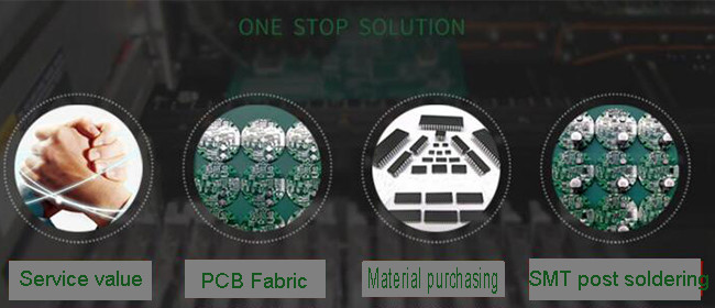
| Service: | One-stop Service,PCB&PCBA,ODM/OEM |
| supplier type: | factory |
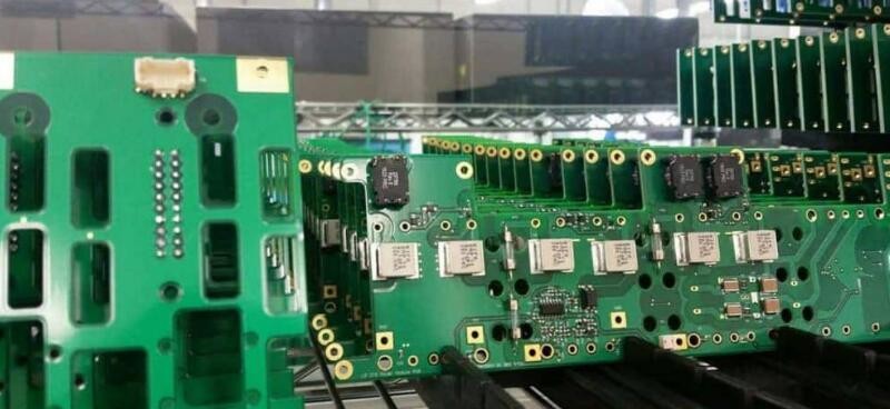
Prototype Printed Circuit Board Assembly as fast as 24 hours.
We use the Latest Technology in SMT & Through-Hole Equipment.
No Set-up Fees, No Minimum Quantity, On Time Delivery.
Prototype printed circuit board (PCB) assemblies also named surface-mount technology (SMT) PCB prototypes, PCBA prototype assembly, PCB sample assembly, etc.
Surface-mount (SMT), through-hole (THT) and mixed-technology components and fine-pitch parts and ball grid arrays (BGAs) for high-density FR-4 PCBs .
| FACTORY CAPABILITIES | |||
| No. | Items | 2019 | 2020 |
| 1 | HDI Capabilities | HDI ELIC (4+2+4) | HDI ELIC(5+2+5) |
| 2 | Max layer count | 32L | 36L |
| 3 | Board Thickness | Core thickness 0.05mm-1.5mm ,Fineshed board thickness 0.3-3.5mm | Core thickness 0.05mm-1.5mm ,Fineshed board thickness 0.3-3.5mm |
| 4 | Min.Hole Size | Laser 0.075mm Mechnical 0.15 | Laser 0.05mm Mechnical 0.15 |
| 5 | Min Line Width/Space | 0.035mm/0.035 | 0.030mm/0.030mm |
| 6 | Copper Thickness | 1/3oz-4oz | 1/3oz-6oz |
| 7 | Size Max Panel size | 700x610mm | 700x610mm |
| 8 | Registration Accuracy | +/-0.05mm | +/-0.05mm |
| 9 | Routing Accuracy | +/-0.075mm | +/-0.05mm |
| 10 | Min.BGA PAD | 0.15mm | 0.125mm |
| 11 | Max Aspect Ratio | 10:1 | 10:1 |
| 12 | Bow and Twist | 0.50% | 0.50% |
| 13 | Impedance Control Tolerance | +/-8% | +/-5% |
| 14 | Daily output | 3,000m2 (Max capacity of equipment) | 4,000m2 (Max capacity of equipment) |
| 15 | Surface Finishing | HASL Lead Free /ENEPING /ENIG /HASL /FINGER GOLD/IMMERSION TIN/SELECTIVE THICK GOLD | |
| 16 | Raw Material | FR-4/Normal Tg/High Tg/Low Dk/HF FR4/PTEE/PI | |
| PCBA Capability | |||
| Material Type | Item | Min | Max |
| PCB | Dimension (length,width,height.mm) | 50*40*0.38 | 600*400*4.2 |
| Material | FR-4,CEM-1,CEM-3,Aluminium-based board,Rogers,ceramic plate,FPC | ||
| Surface finish | HASL,OSP,Immersion gold,Flash Gold Finger | ||
| Components | Chip&IC | 1005 | 55mm |
| BGA Pitch | 0.3mm | - | |
| QFP Pitch | 0.3mm | - | |
| Product Type | Qty | Normal lead time | Quick-turn lead time |
| SMT+DIP | 1-50 | 1WD-2WD | 8H |
| SMT+DIP | 51-200 | 2WD-3WD | 1.5WD |
| SMT+DIP | 201-2000 | 3WD-4WD | 2WD |
| SMT+DIP | ≥2001 | 4WD-5WD | 3WD |
| PCBA(2-4Layer) | 1-50 | 2.5WD-3.5WD | 1WD |
| PCBA(2-4Layer) | 51-2000 | 5WD-6WD | 2.5WD |
| PCBA(2-4Layer) | ≥2001 | ≥7WD | 5WD |
| PCBA(6-10Layer) | 1-50 | 3WD-4WD | 2.5WD |
| PCBA(6-10Layer) | 51-2000 | 7WD-8WD | 6WD |
| PCBA(10-HDILayer) | 1-50 | 7WD-9WD | 5WD |
| PCBA(10-HDILayer) | 51-2000 | 9WD-11WD | 7WD |
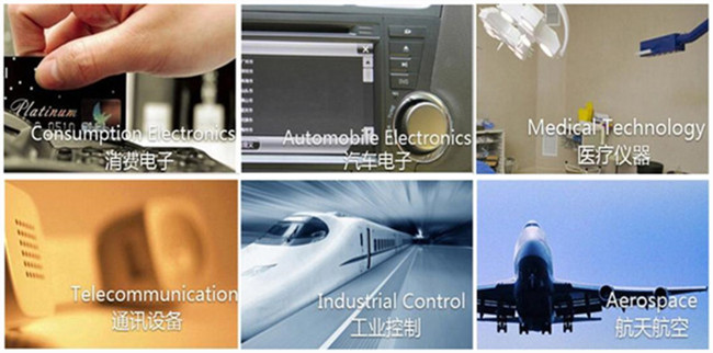
At present, the main cooperation industries are automotive
electronics, communications, consumer electronics, medical equipment, audio and video, optoelectronics, robotics, hydroelectric power,
medical care, aerospace, education, radio frequency, power supply,
printer etc industries.
Market Success:
Products are mainly exported to Europe and USA;
Our customers spread over more than 80 countries;
Products are widely used in various industries.
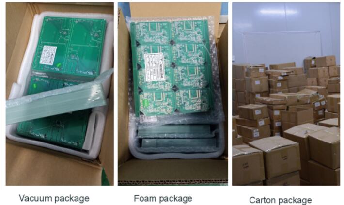
PCB: Vacuum packaging with carton box
PCBA: ESD packaging with carton box
1.What are needed for quotation?
PCB: Quantity, Gerber file and Technic
requirements(material,surface finish treatment, copper
thickness,board thickness ......)
PCBA: PCB information, BOM, (Testing documents...)
2. What file formats do you accept for production?
Gerber file: CAM350 RS274X
PCB file: Protel 99SE, P-CAD 2001 PCB
BOM: Excel (PDF,word,txt)
3.Are my files safe?
Your files are held in complete safety and security.We protect the
intellectual property for our customers in the whole process.. All
documents from customers are never shared with any third party.
4.MOQ?
There is no MOQ .We can flexibly handle small and mass production.
5.Shipping Cost ?
The shipping cost is determined by the destination ,weight ,packing size of the goods .We can provide shipping, air, land, express and other transportation services .
6.How to ensure high-quality production?
The process is strictly controlled under ISO 9001:2015 standards.
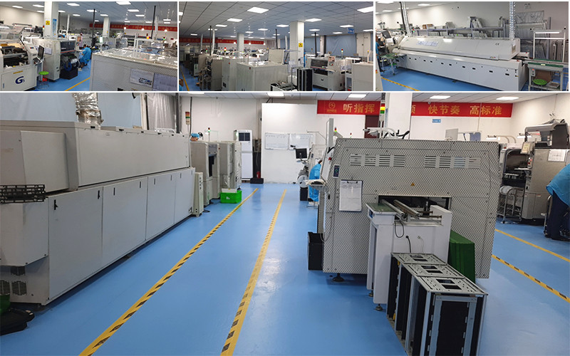
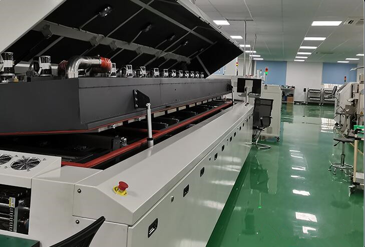
Most of our advanced equipment and tools are imported from abroad.
Such as Flying Probe, X-ray Inspection, AOI (Automated Optical
Inspector) and ICT (in-circuit testing).
We have a very professional QC team.
Q7.What are the services you can provide ?
One-stop contract manufacturing
A:PCB Assembly;
B:PCB Design & Layout
C:PCBA programming & functional testing;
D:Electronic components purchasing service;
E:Enclosure molding & final assembly with
labels,instructions,enclosure, boxes.
Q8.Whether all PCBA s will be tested before delivery ?
Yes , we will test each piece of PCBA product under your testing methods ,to ensure quality and functionality .
Q9.Do you provide OEM service ?
Yes ,we offer PCB and PCBA OEM Service , we manufacture the PCB and PCBA products to your design and requirements .
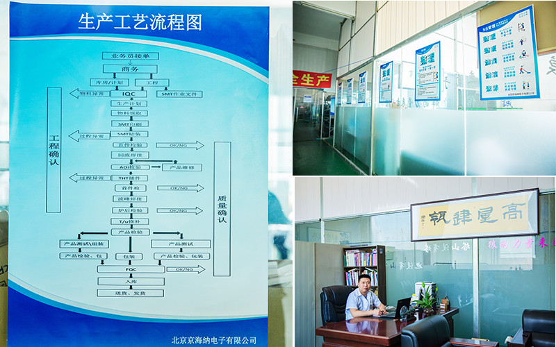
Haina lean Electronics Co., Ltd is a one-stop EMS supplier integrating PCB design, PCB manufacturing, Component sourcing and PCB assembly.
Our company is specialized in electronic products supporting processing services, mainly to undertake circuit board design, layout production, components procurement, PCB plate making, circuit board welding assembly debugging and other OEM/ODM services.
Our first factory is located in Changping District, Beijing, the main radiation Haidian, Changping, Chaoyang three areas of Beijing. We have been adhering to creating high quality, high efficiency, low-cost business philosophy based on the circuit board processing industry for customers.
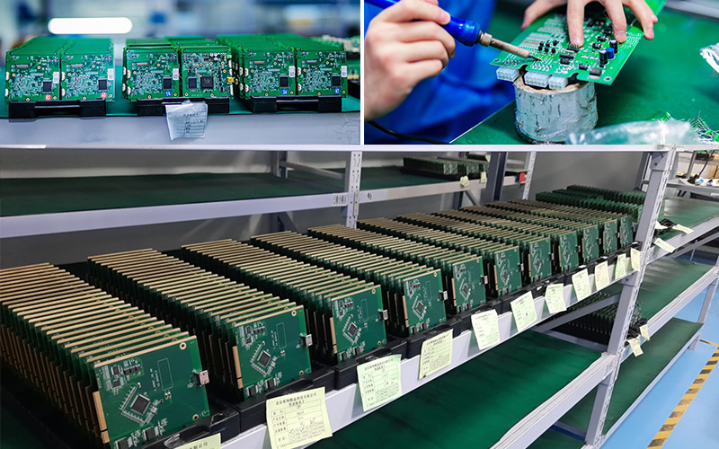
Most of the key staff of the company are mature technical talents who have been engaged in the industry for more than 10 years, and have rich experience in the production of SMT and DIP, also has rich experience in production for high density & difficulty to package components such as BGA. Our second branch plant is located in Langfang city, and mainly cover Fengtai and Daxing Yizhuang area. Totally HAINA LEAN COMPANY covers an area of 6000 square meters. We obtain a good reputation in the industry through the continuous efforts of all staff and high quality service .

|
