| Sign In | Join Free | My frbiz.com |
|
| Sign In | Join Free | My frbiz.com |
|
| Categories | 8 Layer PCB |
|---|---|
| Brand Name: | WITGAIN PCB |
| Model Number: | PCB000332 |
| Certification: | UL |
| Place of Origin: | China |
| MOQ: | 1 pcs/lot |
| Price: | negotiable |
| Payment Terms: | T/T |
| Supply Ability: | 100k pcs/month |
| Delivery Time: | 20 days |
| Packaging Details: | Vacuum bubble bag packaging |
| Layer Count: | 8 Layer |
| Material: | FR4 TG 170 |
| PCB Thickness: | 1.6 MM |
| Solder mask colour:: | Black Solder Mask |
| BGA Size: | 8 mil |
| Min Trace: | 3/3 mil |
| Company Info. |
| Witgain Technology Limited |
| View Contact Details |
| Product List |
8 Layer Via In Pad Treatment PCB Black Solder Mask
Main Features:
1 8 Layer Printed Circuit Board with very high relability.
2 PCB drawing size is 142mm*96mm/1pcs
3 Copper thickness is 35 um on each layer
4 FR4 substrate material ,halogen free material.
5 Surface treatment is immersion gold.
6 Gold thickness is 1U'.
7 Finished board thickness is 1.6mm.
8 Gerber file or PCB file should be offered by customer before production.
Our Equipment List:
| NO | Equipment Name | Equipment Brand | Equipment QTY |
| 1 | Automatic Cutting | SCHCLLING-CA6858 | 1 |
| 2 | Roll Cutting | QIXIAN | 2 |
| 3 | Vertical Cutting | SHANGYUE | 2 |
| 4 | Innerlayer pretreatment | JIECHI | 4 |
| 5 | Automatic coat&wiring | QUNYU | 4 |
| 6 | Automatic exposure | CHUANBAO | 11 |
| 7 | Large table exposure | HECHUAN | 2 |
| 8 | Laser Plotter | ORBOTEC | 3 |
| 9 | Etching line | KB | 4 |
| 10 | PE Punching | PE-3000 | 1 |
| 11 | AOI | ORBOTEC | 10 |
| 12 | Double row brown | KB | 3 |
| 13 | PP Cutting | ZHENGYE | 5 |
| 14 | PP Chopping | ZHONGDA | 2 |
| 15 | Hot-melt machine | HANSONG | 6 |
| 16 | Riveting machine | JIAOSHI | 6 |
| 17 | X-Ray Check | HAOSHUO | 5 |
| 18 | Automatic reflux | LANDE | 2 |
| 19 | Steel plate washer | FENGKAI | 2 |
| 20 | Large size press | DATIAN | 8热4冷 |
| 21 | X-Ray Drilling target | HAOSHUO | 8 |
| 22 | Ccd Drilling target | XUELONG | 10 |
| 23 | Automatic grinding | XINHAO | 5 |
| 24 | Plate thickness Measuring | AISIDA | 2 |
| 25 | Four axis gongs machine | DALIANG | 2 |
| 26 | Two axis gongs machine | BIAOTEFU | 4 |
| 27 | Automatic grinding mill | JIEHUI | 2 |
| 28 | Drilling machine | TONGTAI | 13 |
| 29 | Hole testing machine | YAYA | 1 |
| 30 | Sinking rough mill | KB | 1 |
| 31 | Vertical copper wire | YAMEI | 1 |
| 32 | Automatic electroplating line | JINMING | 1 |
| 33 | Dryer after electroplating | KB | 1 |
| 34 | Etch machine | KB | 1 |
| 35 | Film checking machine | YUBOLIN | 2 |
| 36 | Line pre-processing | KB | 2 |
| 37 | Automatic laminator | ZHISHENG | 3 |
| 38 | Outer exposure machine | CHUANBAO | 8 |
| 39 | Outer exposure machine | HECHUAN | 3 |
| 40 | Etch machine | JULONG | 1 |
| 41 | Line developing machine | KB | 1 |
| 42 | Sand blasting machine | KB | 1 |
| 43 | Precoarsening pretreatment | KB | 2 |
| 44 | Electrostatic spraying line | FURNACE | 1 |
| 45 | Automatic screen printing machine | HENGDAYOUCHUANG | 12 |
| 46 | Pre baked tunnel furnace | KB | 1 |
| 47 | Solder resist exposure machine | CHUANBAO | 6 |
| 48 | Solder resist exposure machine | HECHUAN | 2 |
| 49 | Post baked tunnel furnace | GC0-77BD | 2 |
| 50 | Solder resist developing machine | KB | 1 |
| 51 | Screen printing machine | 1.8mm/2.0mm | 4 |
| 52 | Character baking tunnel furnace | GC0-77BD | 1 |
| 53 | Sunk Tin spray line | 2 | |
| 54 | Nickel palladium and gold wire | XINHUAMEI | 1 |
| 55 | Alternator | 2 | |
| 56 | OSP line | KB | 1 |
| 57 | Gongs machine | YIHUI | 20 |
| 58 | V-CUT | ZHENGZHI | 1 |
| 59 | CNC V-CUT machine | CHENGZHONG | 2 |
| 60 | Hydraulic punch press | SRT | 2 |
| 61 | Test machine | MASON | 17 |
| 62 | High speed flying needle tester | WEIZHENGTAI | 3 |
| 63 | Four wire flying needle tester | XIELI | 2 |
| 64 | Product washing machine | KB | 2 |
| 65 | Plate warping machine | XINLONGHUI | 2 |
| 66 | Vacuum packaging machine | SHENGYOU | 4 |
FAQ:
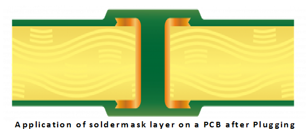
Q1:What is Via plugging? When is it used? How is it different from Via Tenting?
A1: Via plugging is a process in which vias are completely filled with resin or closed with a solder mask. This technique is different from via tenting where resin/solder mask doesn’t fill the via hole but just provides a covering.

Via plugging is done as a preventive measure to secure the vias from the unwanted flow of solder material during the assembly/soldering process. During the soldering process, if a via is not plugged or tented, the solder can flow down the via from the pads and can create unnecessary solder joints.
Via plugging can be done using conductive or non-conductive materials. The conductively filled vias help to carry a large amount of current from one side of the PCB board to another. However, the main drawback of conductively filled vias is the difference in CTE (Coefficient of Thermal Expansion) between the conductive fill and surrounding laminate. During PCB operation, the conductive material will heat and expand at a faster rate than the surrounding laminate, which can cause a fracture between the via wall and associated contact pad.
The via holes filled with non-conductive materials will still function like normal vias. However, they will not be able to carry higher current loads like those filled with conductive materials.

|
