| Sign In | Join Free | My frbiz.com |
|
| Sign In | Join Free | My frbiz.com |
|
| Categories | Rapid PCBA |
|---|---|
| Brand Name: | HNL-PCBA |
| Model Number: | Rapid PCBA |
| Certification: | ISO9001,IS16949, ISO14001,ROHS ,IPC-A ,QC080000 |
| Place of Origin: | CHINA |
| MOQ: | 1 PC |
| Price: | Negotiable |
| Payment Terms: | T/T, Western Union, L/C, MoneyGram |
| Supply Ability: | 10,000,000 Point /Day |
| Delivery Time: | 1-7days |
| Packaging Details: | ESD packaging with carton box |
| Product name: | Rapid PCBA |
| Layers: | Double side ,Multilayer |
| Copper thickness: | 0.3oz 0.6oz 1.0oz 2oz ...... 6oz |
| Min. line spacing / width: | 0.030mm / 0.030mm |
| Board thickness: | 0.3mm-3.5mm |
| Min. hole size: | Laser 0.05mm ; Mechnical 0.15 |
| Solder mask color: | Green,white,black,red,orange,yellow,blue,purple |
| Surface treatment: | OSP,HAL,HAL LF,ENIG,Hard gold,Imm Ag,Imm Sn,Peelable soldermask,Carbon ink print,Selective hard gold |
| Base material: | High Tg FR-4, Halogen Free FR-4, Thick Copper FR-4, Aluminium Based, Rogers, Taconic |
| Application: | Consumer Electronics,Industry/Medical/Consumer electronic,PCBA Circuit Board |
PCBA is the abbreviation of Printed Circuit Board Assembly in
English, that is to say, PCB blank board goes through SMT loading,
or the entire process of DIP plug-in, referred to as PCBA, and the
standard way of writing in Europe and America is PCB'A, with "'"
added, this Known as the official idiom.
| FACTORY CAPABILITIES | |||
| No. | Items | 2019 | 2020 |
| 1 | HDI Capabilities | HDI ELIC (4+2+4) | HDI ELIC(5+2+5) |
| 2 | Max layer count | 32L | 36L |
| 3 | Board Thickness | Core thickness 0.05mm-1.5mm ,Fineshed board thickness 0.3-3.5mm | Core thickness 0.05mm-1.5mm ,Fineshed board thickness 0.3-3.5mm |
| 4 | Min.Hole Size | Laser 0.075mm Mechnical 0.15 | Laser 0.05mm Mechnical 0.15 |
| 5 | Min Line Width/Space | 0.035mm/0.035 | 0.030mm/0.030mm |
| 6 | Copper Thickness | 1/3oz-4oz | 1/3oz-6oz |
| 7 | Size Max Panel size | 700x610mm | 700x610mm |
| 8 | Registration Accuracy | +/-0.05mm | +/-0.05mm |
| 9 | Routing Accuracy | +/-0.075mm | +/-0.05mm |
| 10 | Min.BGA PAD | 0.15mm | 0.125mm |
| 11 | Max Aspect Ratio | 10:1 | 10:1 |
| 12 | Bow and Twist | 0.50% | 0.50% |
| 13 | Impedance Control Tolerance | +/-8% | +/-5% |
| 14 | Daily output | 3,000m2 (Max capacity of equipment) | 4,000m2 (Max capacity of equipment) |
| 15 | Surface Finishing | HASL Lead Free /ENEPING /ENIG /HASL /FINGER GOLD/IMMERSION TIN/SELECTIVE THICK GOLD | |
| 16 | Raw Material | FR-4/Normal Tg/High Tg/Low Dk/HF FR4/PTEE/PI | |
| PCBA Capability | ||||||
| Material type | PCB | Components | ||||
| Item | Dimension (Length, width,height. mm) | Material | Surface finish | Chip&IC | BGA Pitch | QFP Pitch |
| Min | 50*40*0.38 | FR-4,CEM-1,CEM-3,Aluminium-based board,Rogers,ceramic plate,FPC | HASL, OSP, Immersion gold, Flash Gold Finger | 1005 | 0.3mm | 0.3mm |
| Max | 600*400*4.2 | |||||
Our service
PCB Design & Layout
PCB Prototyping
PCB Fabrication
Turn Prototype PCB Assembly
PCB Assembly Services
PCBA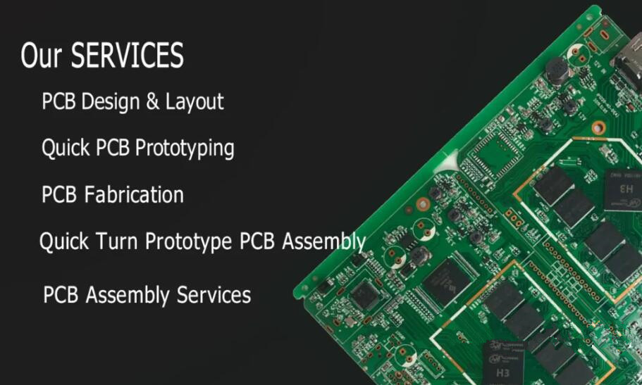
AL-SPI-IA
solder paste printing equipment
wave-soldering
automatic printing equipment
60times magnifying glass
material baking equipment
X-ray welding inspection
Semi-automatic printing equipment
component counting equipment
Online AOI detector
Reflow welding equipment
Mydata welding equipment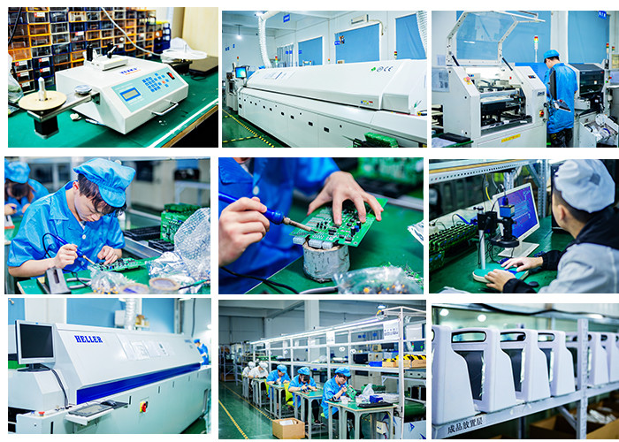
Printed circuit boards And PCB Assembly are mainly used for many
communication industry, medical equipments, consumer electronics
,automotive electronics , Elevator,audio and video, optoelectronics, robotics, hydroelectric power, Elevator,aerospace, education, power supply, printer ,Auto Industry ,Smart
Home.etc.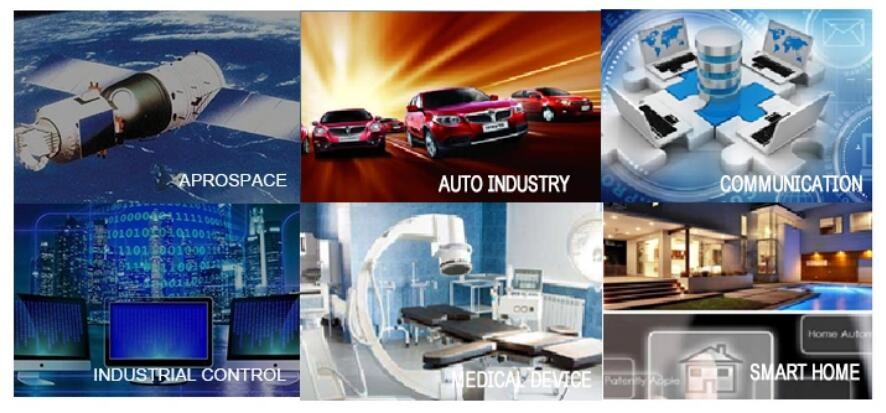
| Product Type | Qty | Normal lead time | Quick-turn lead time |
| SMT+DIP | 1-50 | 1WD-2WD | 8H |
| SMT+DIP | 51-200 | 2WD-3WD | 1.5WD |
| SMT+DIP | 201-2000 | 3WD-4WD | 2WD |
| SMT+DIP | ≥2001 | 4WD-5WD | 3WD |
| PCBA(2-4Layer) | 1-50 | 2.5WD-3.5WD | 1WD |
| PCBA(2-4Layer) | 51-2000 | 5WD-6WD | 2.5WD |
| PCBA(2-4Layer) | ≥2001 | ≥7WD | 5WD |
| PCBA(6-10Layer) | 1-50 | 3WD-4WD | 2.5WD |
| PCBA(6-10Layer) | 51-2000 | 7WD-8WD | 6WD |
| PCBA(10-HDILayer) | 1-50 | 7WD-9WD | 5WD |
| PCBA(10-HDILayer) | 51-2000 | 9WD-11WD | 7WD |
Partners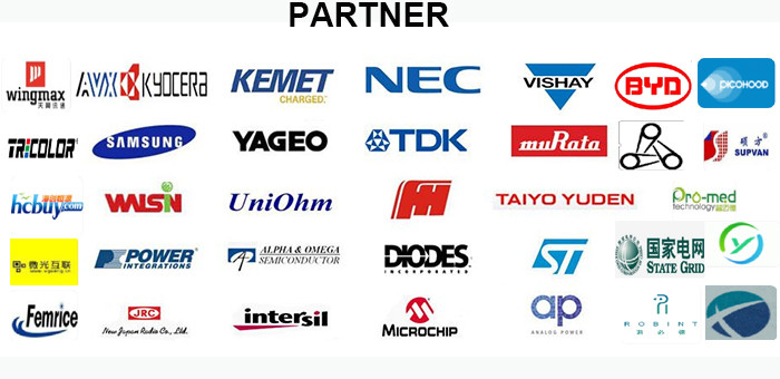
PCB: Vacuum packaging with carton box
PCBA: ESD packaging with carton box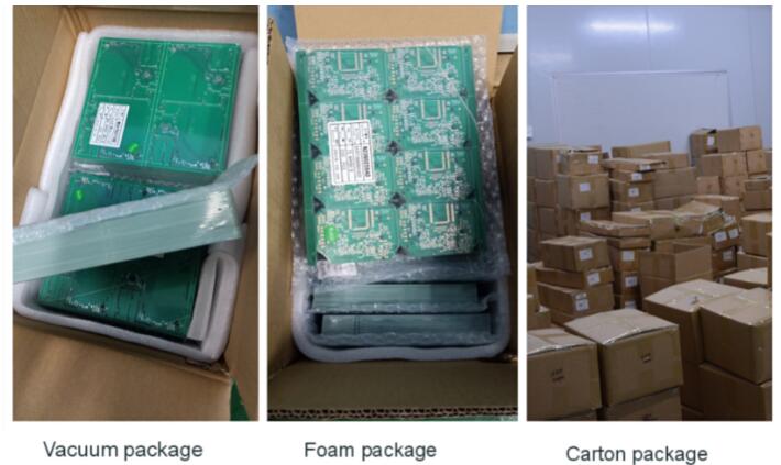
FAQ
1, What service do you provide?
We provide turnkey solution including PCB fabrication, SMT Process,
PCB Assembly,final assembly, Function testing and other value-added
service.
2, What is needed for PCB & PCBA quotation?
PCB: Quantity, Gerber file and technic requirements(material,size,
surface finish treatment, copper thickness,board thickness).
PCBA: PCB information, BOM,Testing documents.
3, How to keep our product information and design file secret ?
We can sign a NDA effect by customers side local law and promising
to keep customers data in high confidential level.
4, What are the main products of your PCB/PCBA services?
Automotive, Medical, Industry Control,IOT,Smart Home,Military.
5, What is your minimum order quantity (MOQ)?
Our MOQ is 1 PCS, sample and mass production all can support.
6.What are the services you can provide ?
One-stop contract manufacturing
A:PCB Assembly;
B:PCB Design & Layout
C:PCBA programming & functional testing;
D:Electronic components purchasing service;
E:Enclosure molding & final assembly with
labels,instructions,enclosure, boxes.
7.Whether all PCBA s will be tested before delivery ?
Yes , we will test each piece of PCBA product under your testing
methods ,to ensure quality and functionality .
8.Do you provide OEM service ?
Yes ,we offer PCB and PCBA OEM Service , we manufacture the PCB and
PCBA products to your design and requirements .
9. Do you accept process materials supplied by clients?
A Yes, we can provide component source, and we also accept
component from client
Company Information
Haina lean Electronics Co., Ltd is one of the most professional PCB
manufacture in Beijing,China.With 8 years of development, Haina
Lean Electronics turns into a first class manufacture of HDI PCB
,with production capability 4000 square meters.
Haina Lean Electronics is providing high quality bare PCB,PCB
layout design service and PCB assembly service,including components
sourcing, function test,conformal coating and complete assembly for
clients all.
We have profuse experience in manufacturing PCB,owned experienced
technical R & D technology team, young and professional sales and
customer service team, experienced and professional procurement
team and assembly testing team, which make sure the products
quality of the pass rate, on-time delivery rate of customer orders.
Our services include: circuit board design and layout, 2-46 layers
PCB manufacturing, professional FPC production, electronic
components purchasing, SMT professional processing, Soldering and
Assembly, especially sample and small bulk orders. we have the
advantages of a quick quote, fast production, fast delivery.

|
