| Sign In | Join Free | My frbiz.com |
|
| Sign In | Join Free | My frbiz.com |
|
| Categories | Double Side PCB Assembly |
|---|---|
| Brand Name: | HNL-PCBA |
| Model Number: | Double Side PCB Assembly |
| Certification: | ISO9001,IS16949, ISO14001,ROHS ,IPC-A , UL, QC080000 |
| Place of Origin: | CHINA |
| MOQ: | 1 PC |
| Price: | Negotiable |
| Payment Terms: | T/T, Western Union, L/C, MoneyGram |
| Supply Ability: | 10,000,000 Point /Day |
| Delivery Time: | 1-7days |
| Packaging Details: | ESD packaging with carton box |
| Product name: | Double Sided PCB Manufacturing Process |
| Number of layers: | Custom |
| Copper thickness: | 0.3oz 1oz 2oz 3 oz ..... 6oz |
| Min. line spacing: | 0.030mm ,0.03mm |
| Board thickness: | 0.3mm 1.2mm 1.6mm , ,,,,,, 3.5mm |
| Min. hole size: | Laser 0.05mm ; Mechnical 0.15 |
| Solder mask color: | Blue.green.red.black.white.etc |
| Material: | FR4 /Normal Tg/High Tg/Low Dk/HF FR4/PTEE/PI |
| Surface finishing: | HASL lead free/ENIG /HASL /FINGER GOLD/IMMERSION TIN/SELECTIVE THICK GOLD |
| Application: | Communication equipment, industrial control, consumer electronics, medical equipment, aerospace,etc. |
Double sided PCB is very similar to single sided PCBs, It has two sided traces with a top and bottom layer.These boards can mount conductive copper and components on both sides of the circuit board, which allows the traces to cross over each other. This results in a higher density of circuits without the need of point-to-point soldering.As these types of circuit boards are more complex than single sided PCBs, it can be more difficult to produce.However, the benefits of using double sided PCBs far outweigh the cons.
| No. | Items | |
| 1 | HDI Capabilities | HDI ELIC(5+2+5) |
| 2 | Max layer count | 36L |
| 3 | Board Thickness | Core thickness 0.05mm-1.5mm ,Fineshed board thickness0.3-3.5mm |
| 4 | Min.Hole Size | Laser 0.05mm Mechnical 0.15 |
| 5 | Min Line Width/Space | 0.030mm/0.030mm |
| 6 | Copper Thickness | 1/3oz-6oz |
| 7 | Size Max Panel size | 700x610mm |
| 8 | Registration Accuracy | +/-0.05mm |
| 9 | Routing Accuracy | +/-0.05mm |
| 10 | Min.BGA PAD | 0.125mm |
| 11 | Max Aspect Ratio | 10:1 |
| 12 | Bow and Twist | 0.50% |
| 13 | Impedance Control Tolerance | +/-5% |
| 14 | Daily output | 4,000m2 (Max capacity of equipment) |
| 15 | Surface Finishing | ENEPING /ENIG /HASL /FINGER GOLD/IMMERSION TIN/SELECTIVE THICK GOLD |
| 16 | Raw Material | FR-4/Normal Tg/High Tg/Low Dk/HF FR4/PTEE/PI |
| PCBA Capability | ||||||
| Material type | PCB | Components | ||||
| Item | Dimension (Length, width,height. mm) | Material | Surface finish | Chip&IC | BGA Pitch | QFP Pitch |
| Min | 50*40*0.38 | FR-4,CEM-1,CEM-3,Aluminium-based board,Rogers,ceramic plate,FPC | HASL, OSP, Immersion gold, Flash Gold Finger | 1005 | 0.3mm | 0.3mm |
| Max | 600*400*4.2 | |||||
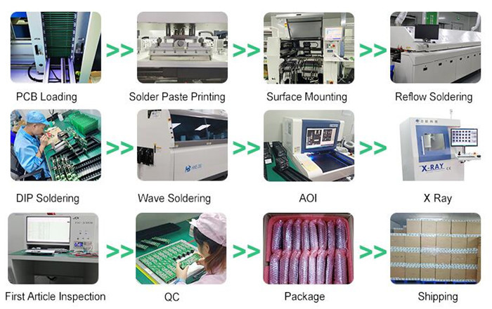
PCB Assembly Process
1.Solder Paste stenciling---2.Surface Mount Technology (Pick and Place)---3.Reflow Soldering---4.Inspection and Quality Control---5.Through-Hole Component Insertion (DIP Process)---6.Final Inspection and Functional Test
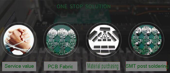
1.Service value
Independent quotation system to quickly serve the market
2.PCB manufacturing
High-tech PCB and PCB assembly production line
3.Material purchasing
A team of experienced electronic component procurement engineers
4.SMT post soldering
Dust-free workshop, high-end SMT patch processing
1. We are the manufacturer/ factory; Welcome to visit us one day.
2. We have good quality control systems, including AOI, ISO 9001 etc. ;
3. All the material we use have the RoHS identify;
4. All the components we use are the New & Original;
5. One-stop service can be provided from PCB design, 1-36 layers PCB manufacturing, components sourcing, PCB Assembly, to Fully Product Assembly.
Printed circuit boards And PCB Assembly are mainly used for many communication industry, medical equipments, consumer electronics and automobile industry ,automotive electronics , audio and video, optoelectronics, robotics, hydroelectric power, aerospace, education, power supply, printer etc industries.

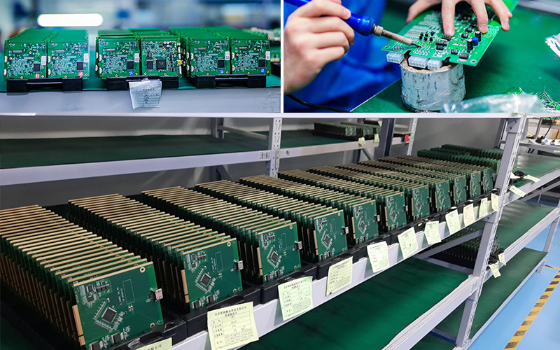
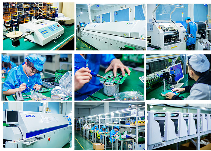
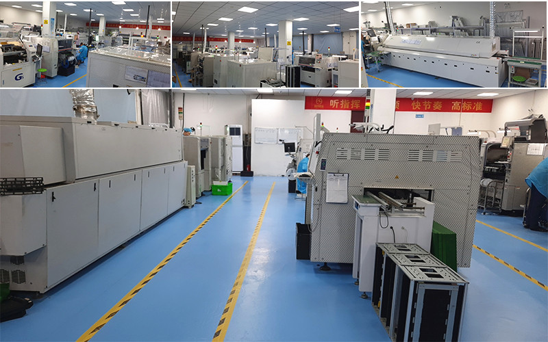
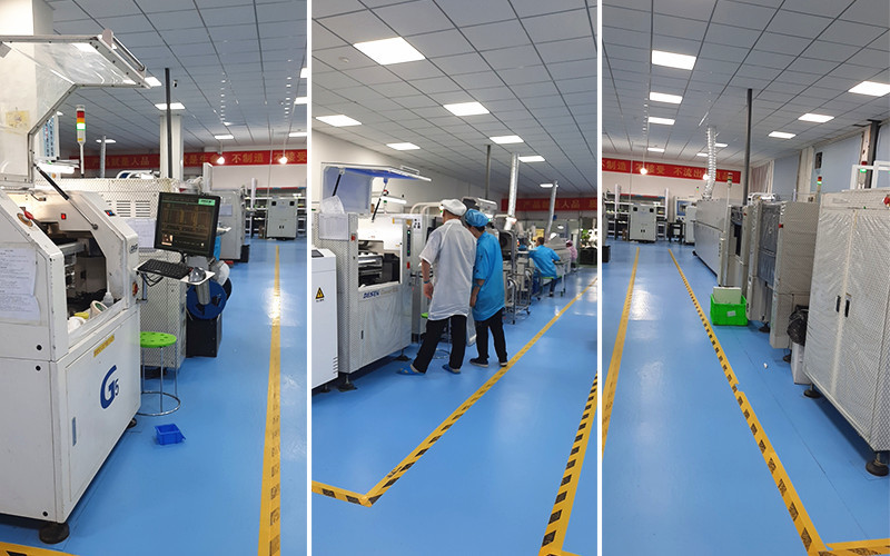
Workshop
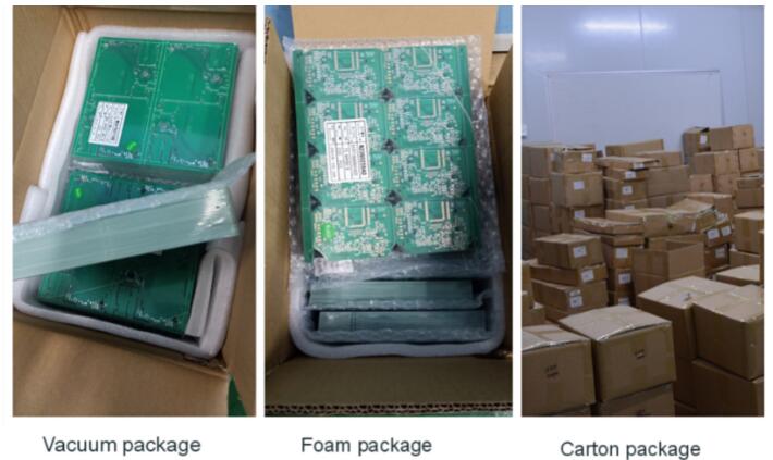
1.PCB: Vacuum packaging with carton box
2.PCBA: ESD packaging with carton box

|
