| Sign In | Join Free | My frbiz.com |
|
| Sign In | Join Free | My frbiz.com |
|
| Categories | Smart Prototyping PCB |
|---|---|
| Model Number: | 020 |
| Place of Origin: | Guangdong, China |
| Packaging Details: | 1.Inner:PCBA: Vacuum Packing 2.Outer: Standard export carton 3.Customized package. |
| Supply Ability: | 80000piece/month |
| Price: | To be negotiated |
| Brand Name: | GUYLAND |
| Certification: | ISO9001 |
| MOQ: | 1000 pieces |
| Delivery Time: | 30-40days |
| Payment Terms: | TT |
| Application: | Smart Home |
| Copper thickness: | 1oz~3oz |
| Base material: | FR-4/aluminum/ceramic/cem-3/FR-1 |
| Board thickness: | 1.6mm |
| Service: | EMS/OEM |
| Layer: | 16 Layer |
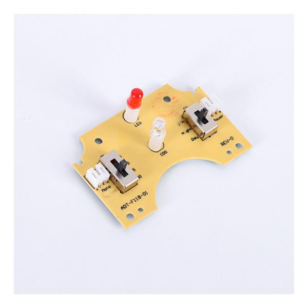
Pcb Top Quality Electronic Assembly Pcb Pure Sine Wave Inverter Pcb Circuit Board Supplier
| Article | Description | Capability |
| Material | Laminate materials | FR4, High TG FR4, High Frequency, Alum, FPC... |
| Board Cutting | Number of layers | 1-48 |
| Min.thickness for inner layers (Cu thickness are excluded) | 0.003”(0.07mm) | |
| Board Thickness | Standard | (0.1-4mm±10%) |
| Min. | Single/Double:0.008±0.004” | |
| 4layer:0.01±0.008” | ||
| 8layer:0.01±0.008” | ||
| Bow and twist | no more than 7/1000 | |
| Copper Weight | Outer Cu weight | 0.5-4 0z |
| Inner Cu weight | 0.5-3 0z | |
| Drilling | Min size | 0.0078”(0.2mm) |
| Drill deviation | ±0.002″(0.05mm) | |
| PTH hole tolerance | ±0.002″(0.005mm) | |
| NPTH hole tolerance | ±0.002″(0.005mm) | |
| Solder Mask | Color | Green,white,black,red,blue… |
| Min solder mask clearanace | 0.003″(0.07mm) | |
| Thickness | (0.012*0.017mm) | |
| Silkscreen | Color | white,black,yellow,blue… |
| Min size | 0.006″(0.15mm) | |
| Max Size of Finish Board | 700*460mm | |
| Surface Finish | HASL,ENIG,immersion silver,immersion tin,OSP… | |
| PCB Outline | Square,circle,irregular(with jigs) | |
| Package | QFN,BGA,SSOP,PLCC,LGA | |


1. Q: Are you manufacturer or trade company?
A: We are the Manufacturer.
2. Q: How can I get the samples? Can you send free samples?
A: We appreciated that you can accept to pay the sample cost and sample freight.
3. Q: When's the delivery time for the sample?
A: The samples will be ready for 7~15 days.
4. Q: Do you offer OEM&ODM service?
A: Yes, we do.
5. Q: When's the delivery time for the order?
A: 10days for small orders , for bulk order , 20-25days days after the receipt of deposit. ltis up to your order quantity and product BOM. 6.Q:What is your minimum order quantity?
A: At least 100pcs for each item,different product different MOQ.
7. Q: What is your payment term?
A: T/T(50% before production and 50% before shipment)
8. Q: What is your shipping ways?
A: For sample we usually send by DHL,FEDEX,UPS,THT,EMS(taking 5-7businessdays). For bulk production we shipping by sea or by air. 9.Q: How do your factory control quality?
A: Quality is the most important part for us. In order to control quality better, We have pro-fessional QC.All our products pass 4 times inspection by QC before delivery.

|
