| Sign In | Join Free | My frbiz.com |
|
| Sign In | Join Free | My frbiz.com |
|
| Categories | Electronics PCB Design |
|---|---|
| Brand Name: | YDY |
| Model Number: | P-011 |
| Certification: | ISO13485, IATF16949, ISO9001 |
| Place of Origin: | China |
| MOQ: | 1pcs |
| Price: | Negotiatable |
| Payment Terms: | L/C, D/A, D/P, T/T, Western Union, MoneyGram |
| Supply Ability: | 100000/month |
| Delivery Time: | 1-5 working days |
| Packaging Details: | Anti-static bag + white pearl cotton (used around the inside of the carton) + carton |
| Name: | Bare board Controlled Impedance Copper coin technology Electronics PCB Design |
| Board Thickness: | Single/Double:0.008±0.004 |
| Min. line width: | 0.1 0mm |
| Min. hole size: | 0.20mm |
| Surface finishing: | ENIG,OSP |
| Copper thickness: | 1~2oz |
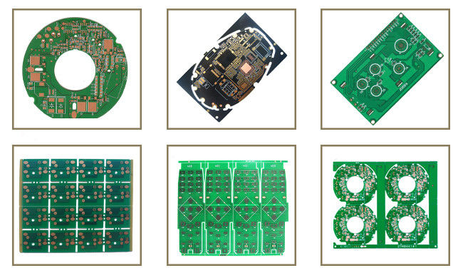
Bare board Controlled Impedance Copper coin technology Electronics PCB Design
Our in house DFM checking process and careful selection of the manufacturing facility, ensures all areas of build and material are covered from fast turn prototypes, some as quick as 24 hours, to volume production
including:
Single Sided.
Double Sided.
Multi Layer
Microvia.
FR4
Polyimide
Flex and Flex Rigid.
Metal Backed
Microwave/RF. (PTFE)
Controlled Impedance.
Backplanes
Complex HDI builds including laser drilled blind and buried
microvias
PCB capability:
| Product Name | Electronics PCB Design |
| Type | Rigid |
| Material | FR4, CEM1, CEM3, High Frequency Board, |
| Layer | 1,2,4,6...20Layer |
| Shape | Retangular, Round, Slots, Cutouts, Complex, Irregular |
| Cutting | Shear, V-score, Tab-routed |
| Board Thickness | 0.2-4mm, regular 1.6mm |
| Copper Thickness | 0.5-4oz, regular 1oz |
| Silk Screen | White, Black, etc. |
| Silk Screen Min Line Width | 0.006" or 0.15mm |
| Min Trace/Gap | 0.1mm or 4mils |
| Min Drill Hole Diameter | 0.01",0.25mm or 10mils |
| Surface Finish | HASL, ENIG, OSP, etc. |
Our capabilities range from large fine pitch QFPs down to 0201 devices and BGAs down to 0.3mm pitch. Our Automated Optical Inspection (AOI) equipment can test components down to 1005. We also offer a BGA inspection, rework and reballing service, using the latest inspection and rework equipment. We offer a fully RoHS compliant service as well as non RoHS for those industries that are currently exempt.

Our in house assembly department offers fast turnaround prototype and pre-production assembly, as well as production runs into the thousands.
Shenzhen Yideyi Technology Co., Ltd have a full final box build facility, capable of building and testing complex final assemblies.
FAQ:
Q1. How can we ensure our information should not let third party to
see our design?
We are willing to sign NDA effect by customer side local law and
promising to keep customers date in high confidential level in all
projects.
Q2. How long does it take for PCB and PCBA Quote ?
PCBs quotation within 2 hours can finished the PCBA depend on the
components
quantity,if simple, within 6 hours can finished,once complex and
more,the 12- 36 hours
can be finished.
Q3. Please note that the following detail will speed up evaluation:
Material:
Board thickness:
Copper thickness:Surface finish:
Solder mask color:
Silkscreen color:
Q4. How about the delivery?
Normally, for sample order, our delivery is about 5 days.For small
batch, our delivery is about 7 days.
For mass production batch, our delivery is about 10 days.
But that depends on the real condition when we get your order.
If your order is urgently please contact us directly ,we will
priority to deal it and do ourbest to give you satisfied delivery
time.
Q5. With payment terms do we accept?
For sample order or small batch, we suggest you to use Pay-pal and
Western Union.For mass production batch, we suggest you to use T/T.
Q6. How can we guarantee you receive an good quality product?
For PCB, we will use Flying Probe Test, E-test etc. for it.
For PCBA, we need you to offer us a method or test fixture for the
function test.Before that, our inspectors will use microscope and
X-ray to check the IC footwelding or bad solder etc.

|
