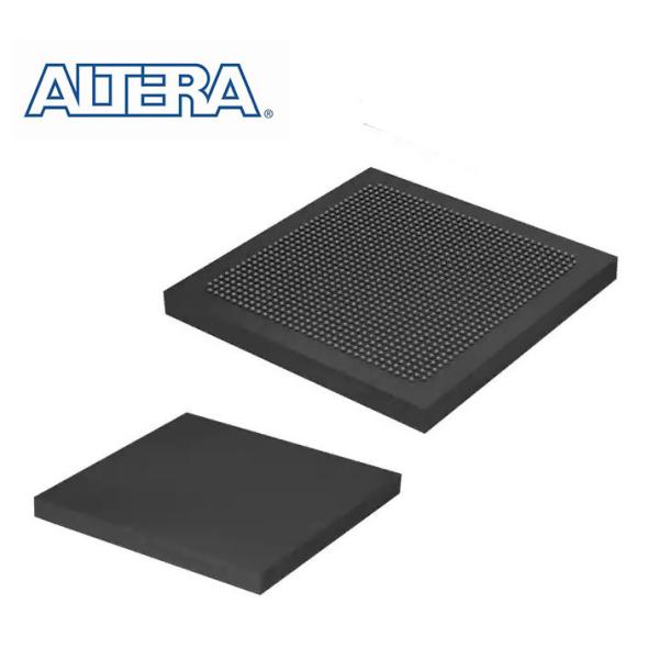
EP3SE260F1152I3N ALTERA FPGA Chip FBGA-1152 Stratix III Enhanced
Product Attribute
Attribute Value
Intel
FPGA - Field Programmable Gate Array
Stratix III Enhanced
255000
10200
744 I/O
1.2 V to 3.3 V
- 40 C
+ 85 C
SMD/SMT
FBGA-1152
Tray
Series:
Stratix III
Brand:
Intel / Altera
Embedded Block RAM - EBR:
1594 kbit
Moisture Sensitive:
Yes
Product Type:
FPGA - Field Programmable Gate Array
Factory Pack Quantity:
24
Subcategory:
Programmable Logic ICs
Total Memory:
16282 kbit
Tradename:
Stratix
Part # Aliases:
972418
Stratix III devices offer the following features:
■ 48,000 to 338,000 equivalent logic elements (LEs) ( refer to
Table 1–1) ■ 2,430 to 20,497 Kbits of enhanced TriMatrix memory consisting of
three RAM block sizes to implement true dual-port memory and FIFO
buffers ■ High-speed DSP blocks provide dedicated implementation of 9×9,
12×12, 18×18, and 36×36 multipliers (at up to 550 MHz),
multiply-accumulate functions, and finite impulse response (FIR)
filters ■ I/O:GND:PWR ratio of 8:1:1 along with on-die and on-package
decoupling for robust signal integrity ■ Programmable Power Technology, which minimizes power while
maximizing device performance ■ Selectable Core Voltage, available in low-voltage devices (L
ordering code suffix), enables selection of lowest power or highest
performance operation ■ Up to 16 global clocks, 88 regional clocks, and 116 peripheral
clocks per device ■ Up to 12 phase-locked loops (PLLs) per device that support PLL
reconfiguration, clock switchover, programmable bandwidth, clock
synthesis, and dynamic phase shifting ■ Memory interface support with dedicated DQS logic on all I/O
banks ■ Support for high-speed external memory interfaces including DDR,
DDR2, DDR3 SDRAM, RLDRAM II, QDR II, and QDR II+ SRAM on up to 24
modular I/O banks
Chuangxinda Electronics was founded in 2000, we have over 20 years
on electronic components experience.
We uphold the integrity and pragmatic, customer success of the
concept, and gradually established a good reputation and
credibility of international business.
We take advantage of a multi-channel established supply
relationship, providing customers with excellent products, chain
management services, full technical support to meet our customers'
product development and production. Our unremitting efforts,
committed to being your best partner.