| Sign In | Join Free | My frbiz.com |
|
| Sign In | Join Free | My frbiz.com |
|
| Categories | Integrated Circuit Chip |
|---|---|
| Brand Name: | Anterwell |
| Model Number: | 74HC574PW |
| Certification: | new & original |
| Place of Origin: | original factory |
| MOQ: | 20pcs |
| Price: | negotiation |
| Payment Terms: | T/T, Western Union,PayPal |
| Supply Ability: | 5300pcs |
| Delivery Time: | 1 day |
| Packaging Details: | please contact me for details |
| feature 1: | 3-state non-inverting outputs for bus oriented applications |
| feature 2: | 8-bit positive edge-triggered register |
| feature 3: | Common 3-state output enable input |
| feature 4: | Independent register and 3-state buffer operation |
| Output capability: | bus driver |
| Icc category: | MSI |
| Company Info. |
| Anterwell Technology Ltd. |
| View Contact Details |
| Product List |
FEATURES
• 3-state non-inverting outputs for bus oriented applications
• 8-bit positive edge-triggered register
• Common 3-state output enable input
• Independent register and 3-state buffer operation
• Output capability: bus driver
• ICC category: MSI
GENERAL DESCRIPTION
The 74HC/HCT574 are high-speed Si-gate CMOS devices and are pin compatible with low power Schottky TTL (LSTTL). They are specified in compliance with JEDEC standard no. 7A.
The 74HC/HCT574 are octal D-type flip-flops featuring separate D-type inputs for each flip-flop and non-inverting 3-state outputs for bus oriented applications. A clock (CP) and an output enable (OE) input are common to all flip-flops.
The 8 flip-flops will store the state of their individual D-inputs that meet the set-up and hold time requirements on the LOW-to-HIGH CP transition.
When OE is LOW, the contents of the 8 flip-flops are available at the outputs.
When OE is HIGH, the outputs go to the high impedance OFF-state.
Operation of the OE input does not affect the state of the flip-flops.
The “574” is functionally identical to the “564”, but has non-inverting outputs.
The “574” is functionally identical to the “374”, but has a different pinning.
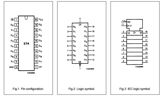
PIN DESCRIPTION
| PIN NO. | SYMBOL | NAME AND FUNCTION |
1 2, 3, 4, 5, 6, 7, 8, 9 10 11 19, 18, 17, 16, 15, 14, 13, 12 20 | OE D0 to D7 GND CP Q0 to Q7 VCC | 3-state output enable input (active LOW) data inputs ground (0 V) clock input (LOW-to-HIGH, edge-triggered) 3-state flip-flop outputs positive supply voltage |

|
