| Sign In | Join Free | My frbiz.com |
|
| Sign In | Join Free | My frbiz.com |
|
| Categories | InSb Wafer |
|---|---|
| Brand Name: | PAM-XIAMEN |
| Place of Origin: | China |
| MOQ: | 1-10,000pcs |
| Payment Terms: | T/T |
| Supply Ability: | 10,000 wafers/month |
| Delivery Time: | 5-50 working days |
| Packaging Details: | Packaged in a class 100 clean room environment, in single container, under a nitrogen atmosphere |
| product name: | Indium Antimonide Substrate Wafer |
| Wafer Diamter: | 3 inch |
| Grade: | Prime Grade |
| feature: | Undoped InSb Wafer |
| Wafer Thickness: | 3″ 800or900±25um |
| keyword: | Indium Antimonide InSb Wafer |
Undoped, Indium Antimonide Substrate, 3”, Prime Grade
PAM-XIAMEN offers InSb wafer – Indium Antimonide which are grown by LEC(Liquid Encapsulated Czochralski) as epi-ready or mechanical grade with n type, p type or undoped in different orientation(111)or(100).Indium antimonide (InSb) is a crystalline compound made from the elements indium (In) and antimony (Sb). It is a narrow-gap semiconductor material from the III-V group used in infrared detectors, including thermal imaging cameras, FLIR systems, infrared homing missile guidance systems, and in infrared astronomy. The indium antimonide detectors are sensitive between 1–5 µm wavelengths.
Undoped, Indium Antimonide Substrate, 3”, Prime Grade
| Wafer Specification | |
| Item | Specifications |
| Wafer Diameter | 3″76.2±0.4mm |
| Crystal Orientation | 3″(111)AorB±0.1° |
| Thickness | 3″ 800or900±25um |
| Primary flat length | 3″22±2mm |
| Secondary flat length | 3″11±1mm |
| Surface Finish | P/E, P/P |
| Package | Epi-Ready,Single wafer container or CF cassette |
| Electrical and Doping Specification | |
| Conduction Type | n-type |
| Dopant | Undoped |
| EPD cm-2 | ≤50 |
| Mobility cm² V-1s-1 | ≥4*105 |
| Carrier Concentration cm-3 | 5*1013-3*1014 |
Band structure and carrier concentration of InSb Wafer include
Basic Parameters,Mobility and Hall Effect,Transport Properties in
High Electric Fields,Impact Ionization
,Recombination Parameters
Basic Parameters
Mobility and Hall Effect
Transport Properties in High Electric Fields
Impact Ionization
Recombination Parameters
| Breakdown field | ≈103 V cm-1 |
| Mobility Electrons | ≤7.7·104 cm2V-1s-1 |
| Mobility Holes | ≤850 cm2V-1s-1 |
| Diffusion coefficient Electrons | ≤2·103 cm2s-1 |
| Diffusion coefficient Holes | ≤22 cm2s-1 |
| Electron thermal velocity | 9.8·105 m s-1 |
| Hole thermal velocity | 1.8·105 m s-1 |
 | Electron Hall mobility versus temperature for different doping levels and different compensation ratios
| |||||||||||||||
 | Electron mobility versus temperature (high temperatures). Solid line is theoretical calculation for electron-drift mobility. Experimental data are Hall mobilities. |
For pure n-InSb at T ≥ 200K:
µnH≈7.7·104(T/300)-1.66 (cm2 V-1 s-1).
 | Electron mobility versus electron concentration. T = 300 K |
 | Electron mobility versus electron concentration. T = 77 K |
 | The electron Hall factor versus carrier concentration. T = 77 K |
| Maximal electron mobility for pure n-InSb | |
| 77 K | 1.2·106 cm2V-1s-1 |
| 300 K | 7.7·104 cm2V-1s-1 |
| Maximal electron mobility for InSb grown on GaAs substrate | |
| 77K | 1.5·105 cm2V-1s-1 (no= 2.2·1015 cm-3) |
| 300 K | 7.0·104 cm2V-1s-1 (no= 2.0·1016 cm-3) |
| Maximal electron mobility for InSb grown on InP substrate | |
| 77 K | 1.1·105 cm2V-1s-1 |
| 300 K | 7.0·104 cm2V-1s-1 |
 | Hole Hall mobility versus temperature for different hole
concentrations. po (cm-3): 1. 8·1014; 2. 3.15·1018; 3. 2.5·1019; |
For pure p-InSb at T > 60K:
µpH≈850(T/300)-1.8 (cm2V-1s-1)
 | Hall mobility versus hole concentrations: 1. 77 K 2. 290K |
 | The hole Hall factor versus carrier concentration, 77 K |
 | Field dependence of the electron drift velocity, 77 K. Solid lines is the Monte Carlo calculation. Points are experimental data. |
 | Field dependence of the electron drift velocity, 77 K. Solid lines is the Monte Carlo calculation. Points are experimental data. |
 | Fraction of electrons in the L-valley as a function of electric
field F, 77K |
 | Frequency dependence of the efficiency in LSA mode Fo = F + F1sin(2π·ft): Fo= 2.5 kV cm-1 |
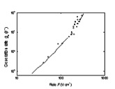 | The dependence of generation rate for electrons gn versus electric
field F, 300 K |
For 300 K, for 30 V/cm < F < 300 V/cm:
gn(F) = 126·F2exp(F/160) (s-1),
where F is in V cm-1.
 | The dependence of generation rate for electrons gn versus electric
field F, 77 K |
 | The dependence of ionization rates for electrons αi versus the
electric field F, T=78 K |
 | The dependence of generation rate for holes gp versus the electric
field F, T =77K |
For pure InSb at T≥250K lifetime of carrier (electrons and holes)
is determined by Auger recombination:
τn = τp ≈1/C ni2,
where C≈5·10-26 cm-6 s-1 is the Auger coefficient.
ni is the intrinsic carrier concentration.
| For T = 300 K | τn = τp≈5·10-8 s |
| For T = 77K | |
| n-type: the lifetime of holes | τp ~ 10-6 s |
| p-type: the lifetime of electrons | τn ~ 10-10 s |
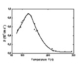
 | Temperature dependence of surface recombination velocity for
p-InSb. |
 | Temperature dependence of surface recombination velocity for
n-InSb. |
| Radiative recombination coefficient | ~5·10-11 cm3s-1 |
| Auger coefficient | ~5·10-26 cm6s-1 |
PAM-XIAMEN is your go-to place for everything wafers, including InSb wafers, as we have been doing it for almost 30 years! Enquire us today to learn more about the wafers that we offer and how we can help you with your next project. Our group team is looking forward to providing both quality products and excellent service for you!

|
