| Sign In | Join Free | My frbiz.com |
|
| Sign In | Join Free | My frbiz.com |
|
| Categories | InSb Wafer |
|---|---|
| Brand Name: | PAM-XIAMEN |
| Place of Origin: | China |
| MOQ: | 1-10,000pcs |
| Payment Terms: | T/T |
| Supply Ability: | 10,000 wafers/month |
| Delivery Time: | 5-50 working days |
| Packaging Details: | Packaged in a class 100 clean room environment, in single container, under a nitrogen atmosphere |
| product name: | P Type InSb Wafer |
| Wafer Diamter: | 2 inch |
| Grade: | Prime Grade |
| feature: | Epi Ready |
| Wafer Thickness: | 2″625±25um |
| keyword: | Indium Antimonide Wafer |
P Type ,LEC InSb(Indium Antimonide) Wafer , 2”, Prime Grade , Epi Ready
PAM-XIAMEN provides single crystal InSb(Indium Antimonide) wafer growth by Liquid Encapsulated Czochralski ( LEC ) method. Indium Antimonide (InSb) can be supplied as wafers with as-cut, etched or polished finishes and are available in a wide range of carrier concentration, diameter and thickness.PAM-XIAMEN can provide epi ready grade InSb wafer for your MOCVD & MBE epitaxial application .
Please contact our engineer team for more wafer information.
P Type, InSb Wafer, 2”, Prime Grade, Epi Ready
| Wafer Specification | |
| Item | Specifications |
| Wafer Diameter | 2″50.5±0.5mm |
| Crystal Orientation | 2″(111)AorB±0.1° |
| Thickness | 2″625±25um |
| Primary flat length | 2″16±2mm |
| Secondary flat length | 2″8±1mm |
| Surface Finish | P/E, P/P |
| Package | Epi-Ready,Single wafer container or CF cassette |
| Electrical and Doping Specification | |
| Conduction Type | p-type |
| Dopant | Genmanium |
| EPD cm-2 | 2″≤100 |
| Mobility cm² V-1s-1 | 8000-4000 |
| Carrier Concentration cm-3 | 5*1014-3*1015 |
Thermal properties of InSb Wafer
| Bulk modulus | 4.7·1011 dyn cm-1 |
| Melting point | 527 °C |
| Specific heat | 0.2 J g-1°C-1 |
| Thermal conductivity | 0.18 W cm-1 °C-1 |
| Thermal diffusivity | 0.16 cm2 s-1 |
| Thermal expansion, linear | 5.37·10-6 °C-1 |
 | Temperature dependence of thermal conductivity n-InSb. Electron
concentration at 78 K n (cm-3): 1. 2·1014; 2. 4.8·1016; 3. 4·1018. Solid line shows the temperature dependence of thermal conductivity at high temperatures |
 | Temperature dependence of thermal conductivity p-InSb. Electron concentration at 78K p (cm-3): 1. 2.7·1014; 2. 5.3·1015; 3. 7.2·1017; 4. 6·1018. |
 | Temperature dependence of specific heat at constant pressure. |
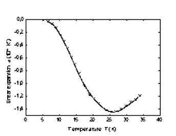 | Temperature dependence of linear expansion coefficient (low
temperatures) |
 | Temperature dependence of linear expansion coefficient (high
temperatures) |
 | Temperature dependence of Sb saturation vapor pressure |
Melting point Tm = 800K.
PAM-XIAMEN is your go-to place for everything wafers, including InSb wafers, as we have been doing it for almost 30 years! Enquire us today to learn more about the wafers that we offer and how we can help you with your next project. Our group team is looking forward to providing both quality products and excellent service for you!

|
